Emerging Memories For IoT And Compute From TSMC, Intel & IBM
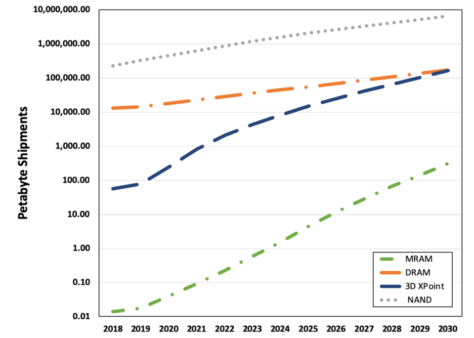
by Tom CoughlinIn earlier blogs I spoke about how new non-volatile memory technologies will be playing an increasing role for embedded and computing applications. In one of my August blogs I mentioned that it appeared that Intel’s Optane memory may finally have reached enough production volume to make it cost effective at the price it must sell at to be competitive with DRAM. The figure below from the Coughlin Associates and Objective Analysis report on Emerging Memories Find Their Direction, shows our projections on the growth of shipped capacity for magnetic random access memory (MRAM) and 3D XPoint (Intel’s Optane memory) as well as more conventional NAND flash and DRAM.

There was evidence of the growing use of MRAM, resistive ram (RRAM) and 3D XPoint memory during presentations at a recent TSMC online technology symposium as well as during the 2020 IEEE Hot Chips Conference. In addition, AI chip company Ambiq announced MRAM in its latest generation Apollo System on Chip (SoC) family. Let’s look at some of these developments.
TSMC had an online technology symposium that I attended where the company where Kevin Zhang talked about their latest developments, including semiconductor technologies at 7, 5 and even 3nm. In addition, the company’s annual report gives some insights on how the company will use emerging non-volatile memory technologies in embedded products.

The company’s annual report says that TSMC’s 22nm resistive RAM (RRAM) started risk production in 2019 and is expected to complete IP reliability qualification in 2020. 40nm RRAM achieved technical qualification as consumer product qualifications continued. TSMC said that there will be multiple customer tape-outs in the second half of 2020. The company’s RRAM is intended for use in low cost internet of things microcontroller MCUs and AI memory devices.
22nm embedded magnetic random access memory (MRAM) technology IPs are expected to complete reliability qualification in 2020. In addition, the company’s 16nm MRAM is under development and is progressing well. Risk production for eFlash-like MRAM is expected in Q421 and SRAM-like MRAM is expected in Q422. The company sees MRAM replacing eFlash in high reliability MCUs, including for AI, IoT and automotive AEC-Q100 Grade-1 applications.
One of TSMC’s customers, Ambiq, is developing chips that will enable the next generation of battery-powered always on voice recognition IoT endpoint devices. The company’s 4th generation Apollo SoC family sets new standards for ultra-low power intelligent endpoint IoT devices. The Apollo 4 is implemented with TSMC’s 22nm ULL process and the 32-bit Arm Cortex-M4 core with floating point unit (FPU) and Arm Artisan physical IP.
The SoC chip achieves power use as low as 3 microA/MHz using MRAM memory with low deep sleep current modes and operates up to 192 MHz clock frequency with TurboSPOT (sub-threshold power-optimized technology), SPOT) and with a 2D/2.5D graphics accelerator and MIPI DSI 1.2 with up to two lanes at 500 Mbps per lane.
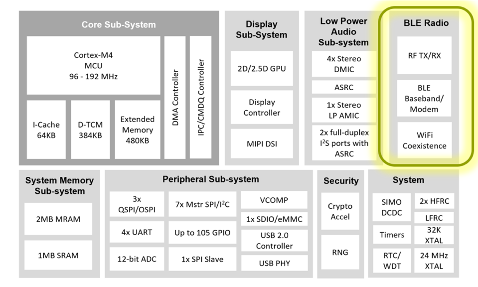
The figure below shows the block diagram showing various features, including 2 MB of MRAM along with up to 1.8 MB of SRAM. The BLE Radio blocks are in the Bluetooth version of the chip.

Ambiq says that the Apollo4 has enough compute and storage resources to handle complex algorithms and neural networks while displaying vibrant, crystal-clear, and smooth graphics. If additional memory is required, external memory is supported through Ambiq’s multi-bit SPI and e.MMC interfaces.
According to Ambiq, the Apollo4 is purpose-built to serve as both an application processor and a coprocessor for battery-powered endpoint devices, including smartwatches, children’s watches, fitness bands, animal trackers, far-field voice remotes, predictive health and maintenance devices, smart security devices, and smart home devices.
The product is targeted for use in intelligent endpoint IoT devices with always-on voice processing.
At the 2020 IEEE Hot Chips Conference there were a few interesting announcements related to emerging memories. Intel gave a talk about their Ice Lake server product where they said that their total memory encryption (TME) encrypts data in DRAM using AES-XTS-128 bit encryption. They also mentioned the use of Intel Optane Persistent 200 series (Barlow Pass) memory.
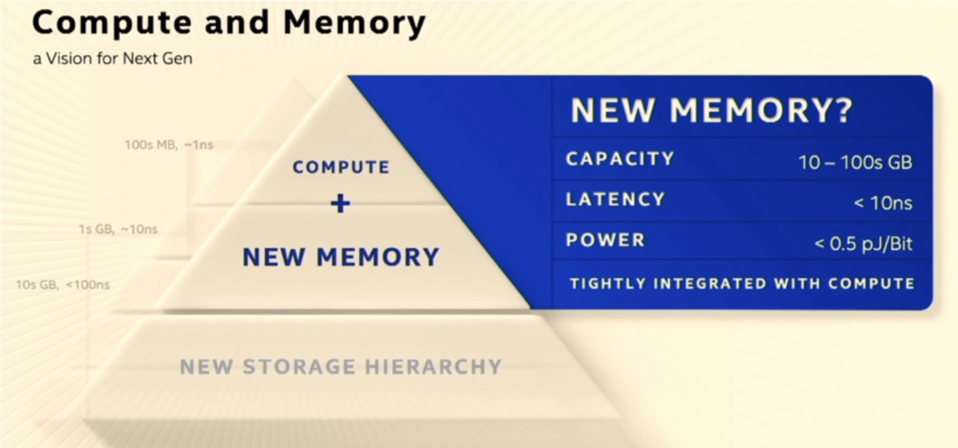
Intel also described latency and coherence optimizations that help the product and make more effective use of memory, including Optane. In particular Intel said they can minimize the impact of persistent memory latencies on performance. Intel also included non-volatile memory as a processor differentiator during a Tiger Lake presentation. There was also mention of the need for new high capacity, low power and low latency memory that is tightly coupled to compute as shown below.

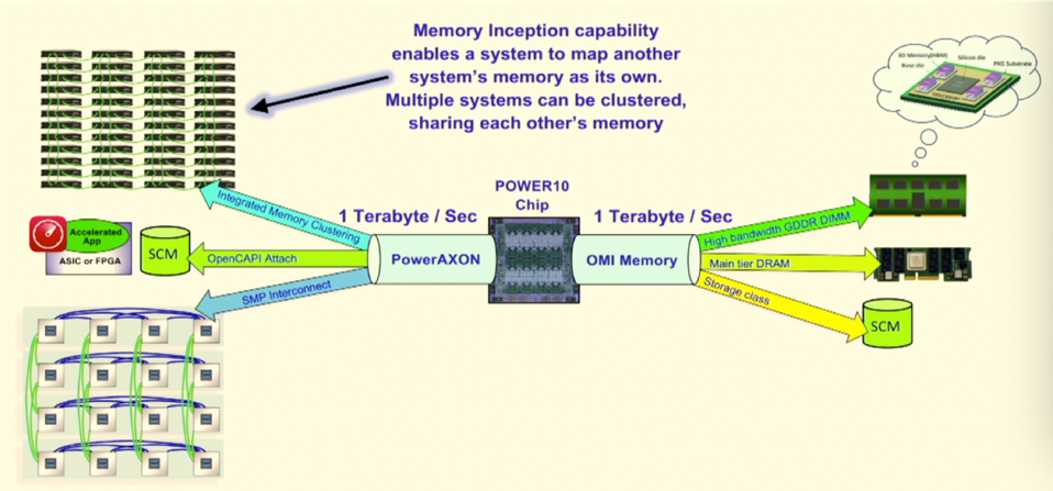
IBM spoke about their latest POWER10 processor for super computer applications (built with Samsung’s 7nm foundry), which included support for non-volatile Storage Class Memory (SCM), similar to Intel’s persistent memory (PM). As shown in the figure below Open Memory interface (OMI) provides high-capacity, encrypted persistent memory in a DIMM slot (likely Optane DIMMs). IBM says that POWER10 can support 2 PB of addressable load/store memory.

IBM also sees high capacity, encrypted persistent SCM attached to FPGAs or ASIC-based accelerators for a POWER10 host with high bandwidth and low latency using open coherent accelerator processor interface (OpenCAPI). POWER10 can also enable a system to map another system’s memory as its own. Multiple systems can be clustered, sharing each other’s memory at Petabyte scale.
Emerging memory for compute, IoT and AI/ML applications was on display at a recent TSMC technical conference, during the Apollo4 SoC announcement by Ambiq and in talks by IBM and Intel at the 2020 IEEE Hot Chips Conference.